Probe Connection Points
Logic analyzer probes were connected to 6 measurement points. Each probe corresponds to a wire colour — this colour coding simplifies signal interpretation.

Differential Signal & Digital Conversion
CAN bus bridges two different signal worlds: the digital signals (0V / 3.3V) that microcontrollers speak, and the differential signals (CAN_H and CAN_L) carried on the physical wire. The transceiver is the bridge between these two worlds.
Digital → Differential
When ESP32 GPIO17 sends a dominant bit (0), the SN65HVD230 pushes both lines in opposite directions simultaneously:
| Line | Recessive (1) | Dominant (0) | Direction |
|---|---|---|---|
| CAN_H | ~2.5V | ~3.5V | ↑ rises by ~1V |
| CAN_L | ~2.5V | ~1.5V | ↓ falls by ~1V |
| CAN_H − CAN_L | ~0V | ~2V | → differential grows to ~2V |
In the recessive state both lines sit at ~2.5V — the difference is near zero. In the dominant state CAN_H rises and CAN_L falls; the ~2V gap between them carries the signal. Because noise affects both lines equally, it cancels out in the differential — this is what makes CAN bus highly noise-resistant.
Differential → Digital
The receiving transceiver measures the CAN_H − CAN_L difference. If the difference exceeds 0.5V → dominant (0); below that threshold → recessive (1). This digital output is then delivered to ESP32 GPIO16 and BBB P9.19.
Optimal Signal Detection Point
Comparing all available measurement points for digital decoding:
| Channel | Recessive | Dominant | Crosses threshold? | Result |
|---|---|---|---|---|
| D0 — CAN_H | ~2.5V | ~3.5V | ✗ always above | Not readable |
| D1 — CAN_L | ~2.5V | ~1.5V | ✓ clearly crosses | Best choice ✓ |
| D2 — ESP32 TX | 3.3V | 0V | ✓ full swing | Readable ✓ |
| D3 — ESP32 RX | 3.3V | 0V | ✓ full swing | Readable ✓ |
| D4 — BBB TX | 3.3V | 0V (ACK only) | ✓ ACK pulse only | Partial |
| D5 — BBB RX | 3.3V | 0V | ✓ full swing | Readable ✓ |
D1 (CAN_L) is the correct detection point for CAN bus decoding with a single-ended logic analyzer. It is the only differential line whose voltage swing reliably crosses the digital threshold in both directions. For true differential measurement of CAN_H, a differential probe and oscilloscope are required.
Signal Propagation — Step by Step
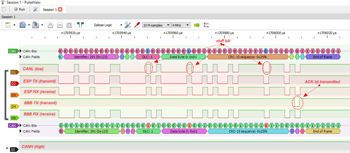
The logic analyzer capture below shows the moment ESP32 transmits a single CAN frame. The progression of the signal across each channel is examined step by step.
ESP32 TX — First bit is placed on the line
When 1 is typed in the Serial Monitor, the ESP32 TWAI driver constructs the frame and begins transmitting it bit by bit from GPIO17. Each bit is held at a fixed voltage for approximately 2 µs (500 kbps → 1 bit = 1/500,000 s = 2 µs). This bit pattern is clearly visible on channel D2.
Transceiver — Digital signal converts to CAN_H / CAN_L
Each bit leaving ESP32 GPIO17 is converted to a differential signal by the SN65HVD230 transceiver. When a dominant bit (0) is transmitted CAN_H rises to ~3.5V and CAN_L falls to ~1.5V. These voltage transitions are observed on channels D0 and D1 — starting simultaneously with D2, with only nanosecond-level propagation delay.
D1, D3, D5 — All receive the same signal simultaneously
The CAN_L line is physically connected to all nodes. Since both ESP32 RX (D3) and BBB RX (D5) are listening on the same wire, the moment the first bit is placed on the line, D1, D3 and D5 show identical waveforms simultaneously. Propagation delay due to cable length is negligible at this scale.
D4 (BBB TX) — Stays silent throughout the frame
BBB is in receiver mode for this frame. Throughout transmission, BBB's TX pin (P9.20 → D4) sends nothing; the line remains silent. Channel D4 reads as a steady HIGH during this period.
ACK slot — BBB pulls dominant, D4 becomes active
Once all frame bits have been transmitted, the CRC field and CRC delimiter follow. Then the ACK slot opens: the transmitter (ESP32) leaves this bit recessive (1). If BBB received the frame without errors, it pulls the line dominant (0) to acknowledge. At exactly this moment a short pulse appears on D4 — this is the ACK bit. ACK DEL and the 7-bit EOF follow; the frame is complete.
CAN Frame Structure — Bit by Bit
Frame decoded from the logic analyzer capture: ID=0x123 · DLC=1 · DATA=0x01 (LED ON) and CRC-15=0x25FE.
| Field | Value | Bits | Description |
|---|---|---|---|
| SOF | 0 | 1 | Start of Frame — dominant bit, all nodes synchronise |
| Identifier | 0x123 (291) | 11 | 00100100011 — standard 11-bit ID, used for bus arbitration |
| RTR | 0 | 1 | Remote Transmission Request — 0 = data frame, 1 = remote request |
| IDE | 0 | 1 | Identifier Extension — 0 = standard (CAN 2.0A), 1 = extended |
| r0 | 0 | 1 | Reserved bit — always 0 |
| DLC | 0001 | 4 | Data Length Code — indicates 1 byte of data |
| Stuff bits | — | +N | Inserted automatically after 5 consecutive identical bits (see S5) |
| Data[0] | 0x01 | 8 | 00000001 — LED ON command |
| CRC-15 | 0x25FE | 15 | Error check sequence — receiver independently calculates and compares this value |
| CRC DEL | 1 | 1 | CRC delimiter — recessive |
| ACK | 0 | 1 | BBB acknowledged by pulling dominant — this is the ACK pulse seen on D4 |
| ACK DEL | 1 | 1 | ACK delimiter — recessive |
| EOF | 1111111 | 7 | End of Frame — 7 recessive bits marking frame completion |
| IFS | 111 | 3 | Intermission — minimum gap between frames |
Bit Stream — Identifier + Control Fields
Stuff Bits — Bit Synchronisation Mechanism
CAN does not use a dedicated clock line. Every node runs on its own clock. In long monotone bit sequences (many consecutive 0s or 1s) the receiver can lose track of bit boundaries. Stuff bits solve this problem.
5 Consecutive Identical Bits → Opposite Stuff Bit Inserted
The receiver removes stuff bits automatically — data integrity is preserved. In the logic analyzer, stuff bits appear highlighted in a distinct colour in the bit stream view.
Error Analysis
Why is the CRC value 0x25FE?
CRC-15 is computed by XOR-ing all bits in the frame (from SOF to the end of the data field, including stuff bits) against the 0x4599 polynomial defined by the CAN standard. Every unique frame content produces a unique CRC.
Two different commands were observed in this capture:
| Command | Data | CRC-15 |
|---|---|---|
| LED ON | 0x01 | 0x25FE |
| LED OFF | 0x00 | 0x6067 |
When the data byte changes by a single bit (0x01 → 0x00) the CRC produces a completely different value. This demonstrates the sensitivity of CRC-15 — even a single-bit error yields a different result, which the receiver will detect.
| Mechanism | Status | Observation |
|---|---|---|
| Bit stuffing | ACTIVE | Stuff bits inserted at DLC→Data transition and within CRC field — synchronisation maintained |
| CRC-15 check | PASSED ✓ | 0x25FE (LED ON) / 0x6067 (LED OFF) — receiver independently computed and verified |
| ACK acknowledgement | RECEIVED ✓ | D4 (BBB TX) produced a dominant pulse at frame end — every frame acknowledged |
| Form check | PASSED ✓ | CRC DEL, ACK DEL, EOF recessive in all frames — no format errors |
| Bit monitoring | PASSED ✓ | ESP32 read back each transmitted bit — no errors detected |
| D4 decoder warning | EXPECTED | "Identifier bits 10..4 must not be all recessive" — D4 carries only the ACK bit, not a full frame |
| Bus state | ERROR-ACTIVE ✓ | Both node error counters at zero — bus healthy |
What We Observed in This Section
- 6 probe points established — CAN_H/L, ESP32 TX/RX, BBB TX/RX
- D1 (CAN_L) selected for decoding — drops below threshold on dominant bits, clean decode
- D0 (CAN_H) cannot be reliably decoded by a logic analyzer — remains above threshold in both states
- D1 ≈ D3 ≈ D5 observed — same physical line, different measurement points
- D4 (BBB TX) active only during the ACK bit — dominant bit principle observed
- Frame decode confirmed: ID=0x123, DLC=1, DATA=0x01, CRC=0x25FE
- Stuff bits observed — bit synchronisation mechanism active
- CRC-15 value is unique to frame content — a single-bit change produces a different CRC
- All CAN error mechanisms passed — system healthy
- Fast Bitrate must be set to 500,000 bps in all decoders (the default 2,000,000 is for CAN FD)
- The D4 decoder warning is expected — it will disappear once BBB transmits full frames